Sequential Elements
CircuitVerse features the following circuit elements in this category:
D Flip Flop
A delay or D Flip Flop circuit element delays the input. As Figure 4.3 shows, it takes in a single data input and a clock input. Some of the other pins include:
-
Preset and Asynchronous Reset: The preset and asynchronous reset pins work in conjunction to change the default behavior of the flip flops.
If Reset = 1, then the D Flip Flop output = Preset: If the asynchronous reset is high, then the output of the flip flop is equal to the value of preset and is independent of the input or the clock. -
Enable: This pin is used to enable the Flip Flop.
As Table 4.12 (the truth table for D Flip Flop) displays, the output of a D Flip Flop is the same as the input data.
Properties that can be customized in the PROPERTIES panel include: BitWidth

Figure 4.3: Pin description of the D Flip Flop within the CircuitVerse platform
Table 4.12: Table for D Flip Flop circuit element
| Clock | D | Q | Q Inverse |
| 0 | X | Latch | Latch |
| 1 | 1 | 1 | 0 |
| 1 | 0 | 0 | 1 |
You can verify the behavior of the D Flip Flop circuit element in the live circuit embedded below:
D Latch
The D Latch circuit element is a single input flip flop. As Figure 4.4, it works similar to a D Flip Flop but it does not include the preset, asynchronous and enable signal pins. The truth table of a D Latch (refer Table 4.13) is similar to that of the D Flip Flop.
Properties that can be customized in the PROPERTIES panel include: BitWidth

Figure 4.4: Pin description of the D Latch within the CircuitVerse platform
Table 4.13: Table for D Latch circuit element
| Clock | D | Q | Q Inverse |
| 0 | X | Latch | Latch |
| 1 | 1 | 1 | 0 |
| 1 | 0 | 0 | 1 |
/* You can verify the behavior of the D Latch circuit element in the live circuit embedded below: [insert live cirucit] */
T Flip Flop
A toggle or T Flip Flop circuit element toggles the output. As Figure 4.5 shows, it takes in a single data input and a clock input. As Table 4.14 (the truth table for T Flip Flop) displays, if the value of the input is 1, then the output of the next state is the complement of the previous state.

Figure 4.5: Pin description of the T Flip Flop within the CircuitVerse platform
Table 4.14: Table for T Flip Flop circuit element
| Input (T) | Previous State | Next State |
| 0 | 0 | 0 |
| 0 | 1 | 1 |
| 1 | 0 | 1 |
| 1 | 1 | 0 |
You can verify the behavior of the **T Flip Flop **circuit element in the live circuit embedded below:
SR Flip Flop
A SR Flip Flop circuit element is one of the simplest sequential circuits. It has two inputs S (stands for “Set”) and R (stands for “Reset”) along with the clock (refer Figure 4.6). As Table 4.15 (the truth table for SR Flip Flop) demonstrates:
- When S is HIGH, the output Q is HIGH.
- When R is HIGH, the output is LOW.

Figure 4.6: Pin description of the SR Flip Flop within the CircuitVerse platform
Table 4.15: Table for SR Flip Flop circuit element
| S | R | Q |
| 0 | 0 | No change |
| 1 | 0 | 1 |
| 0 | 1 | 0 |
| 1 | 1 | Invalid |
You can verify the behavior of the SR Flip Flop circuit element in the live circuit embedded below:
JK Flip Flop
The JK Flip Flop circuit element, an improvement of a SR Flip Flop, includes two inputs J and K along with the clock (refer Figure 4.7). As Table 4.16 (the truth table for a JK flip flop) explains, if the inputs J and K are different, then the output Q takes the value of the input J at the next clock edge.
Properties that can be customized in the PROPERTIES panel include: BitWidth

Figure 4.7: Pin description of the JK Flip Flop within the CircuitVerse platform
Table 4.16: Table for JK Flip Flop circuit element
| J | K | Q |
| 0 | 0 | No change |
| 1 | 0 | 1 |
| 0 | 1 | 0 |
| 1 | 1 | Toggle |
You can verify the behavior of the JK Flip Flop circuit element in the live circuit embedded below:
TTY
A TTY circuit element receives an input sequence of ASCII codes and displays each printable character as output. While Figure 4.8 displays the different pins of TTY, Table 4.17 gives a brief description of the different pins.
Properties that can be customized in the PROPERTIES panel include: BitWidth must be set as 7, Rows, Columns

Figure 4.8: Pin description of the TTY circuit element within the CircuitVerse platform
Table 4.17: Pin description of TTY circuit element within CircuitVerse simulator
| Name | Description |
| ASCII Input (BitWidth 7) | Receives the ASCII value of the next character to be entered into the terminal. |
| Clock (BitWidth 1) | When the clock is triggered and the Enable pin isn't 0, the current ASCII input is processed by the terminal. |
| Enable (BitWidth 1) |
|
| Reset |
|
You can verify the behavior of the TTY circuit element in the live circuit embedded below:
Keyboard
The Keyboard circuit element allows the circuit to read keystrokes, as long as the keystrokes are representable in the seven-bit ASCII code. Figure 4.9 shares the pin description of the Keyboard circuit element and Table 4.18 shares a brief description of the same.
Properties that can be customized in the PROPERTIES panel include: Buffer Size

Figure 4.9: Pin description of the Keyboard circuit element within the CircuitVerse platform
Table 4.18: Pin description of Keyboard circuit element within CircuitVerse simulator
| Name | Description |
| Clock (BitWidth 1) | When the clock is triggered and the Enable pin isn't 0, the leftmost character from the buffer is deleted and the outputs are updated to reflect the buffer's new status. |
| Enable (BitWidth 1) |
|
| Reset |
|
| Available (AVL) |
|
| ASCII Output (BitWidth 7) | Generates the 7-bit ASCII code for the leftmost character in the buffer or 0 if the buffer is empty. |
You can verify the behavior of the Keyboard circuit element in the live circuit embedded below:
Clock
The Clock circuit element toggles its output at regular time intervals.
NOTE: All clocks enabled within a circuit toggle at the same rate.
You can verify the behavior of the Clock circuit element in the live circuit embedded below:
ROM
As the name suggests, the ROM (read-only memory) circuit element stores read only data for computers and other electronic devices. ROM is mostly used for firmware updates. A simple example of ROM is the cartridge used with video game consoles, which allows one system to run multiple games. Another example of ROM is EEPROM, which is a programmable ROM used for the computer BIOS.
The ROM circuit element includes three pins. As Figure 4.10 elucidates, it accepts a 4-bit address input (A) and the corresponding value stored in the particular address is returned as a 8-bit output (D) (initial address always starts from 0). The Enable (En) pin enables the ROM.
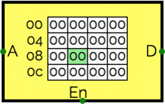
You can verify the behavior of the ROM circuit element in the live circuit embedded below:
RAM
The RAM ( random access memory) circuit element allows data to be read or written. Any changes to Address Width property attribute and BitWidth property attribute will cause data to be lost (refer Figure 4.11). Think of these operations as being equivalent to taking a piece of RAM out of a circuit board and replacing it with another RAM of different size.
Data stored within the RAM can be reset to zero by setting the Reset pin 1 or clicking the Reset button in the PROPERTIES panel. Refer Figure X.
Alternatively, the contents of the RAM can be dumped to the console by transitioning the Core Dump pin to 1 or clicking the Core Dump button in the PROPERTIES panel. Any address spaces that have not been written will show up as undefined in the core dump.
Properties that can be customized in the PROPERTIES panel include: Address Width, BitWidth
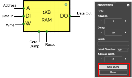
Figure 4.11: RAM circuit element and relevant property attributes available in the PROPERTIES panel
You can verify the behavior of the RAM circuit element in the live circuit embedded below:
EEPROM
The EEPROM circuit element is a programmable ROM used for the computer BIOS. EEPROMs are generally more expensive than RAMs. The maximum address space of the EEPROM circuit element is 10-bits (1024 addresses)––smaller than the RAM. Figure 4.12 shares a pin description of the **EEPROM **circuit element.
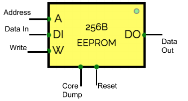
Figure 4.12: EEPROM circuit element available within the CircuitVerse simulator
If the EEPROM is erased, all the values are reset to zero and the original data cannot be recovered. The project can be reloaded for retrieving the saved data.
EEPROM data survives cut-and-paste operations and can be used for different purposes like duplicating EEPROMs, creating an EEPROM in one circuit and then cut-and-pasting the element in another circuit,or create a library of ready-to-use EEPROMs with interesting data.
Properties that can be customized in the PROPERTIES panel include: Address Width, BitWidth
You can verify the behavior of the EEPROM circuit element in the live circuit embedded below:
- To populate the EEPROM, make Write=1 and click Reset to erase everything.
- Click the Keyboard circuit element and type some characters until the address counter in the EEPROM goes back to zero.
- Make Write=0 and the text in the EEPROM will show in the TTY element.
- Save the circuit and it will persist the contents of the EEPROM for future use